Basic Electronics
The goal of this chapter is to provide some basic information about electronic circuits. We make the assumption that you have no prior knowledge of electronics, electricity, or circuits, and start from the basics. This is an unconventional approach, so it may be interesting, or at least amusing, even if you do have some experience. So, the first question is ``What is an electronic circuit?'' A circuit is a structure that directs and controls electric currents, presumably to perform some useful function. The very name "circuit" implies that the structure is closed, something like a loop. That is all very well, but this answer immediately raises a new question: "What is an electric current?" Again, the name "current" indicates that it refers to some type of flow, and in this case we mean a flow of electric charge, which is usually just called charge because electric charge is really the only kind there is. Finally we come to the basic question:
What is Charge?
No one knows what charge really is anymore than anyone knows what gravity is. Both are models, constructions, fabrications if you like, to describe and represent something that can be measured in the real world, specifically a force. Gravity is the name for a force between masses that we can feel and measure. Early workers observed that bodies in "certain electrical condition" also exerted forces on one another that they could measure, and they invented charge to explain their observations. Amazingly, only three simple postulates or assumptions, plus some experimental observations, are necessary to explain all electrical phenomena. Everything: currents, electronics, radio waves, and light. Not many things are so simple, so it is worth stating the three postulates clearly.
Charge exists.
We just invent the name to represent the source of the physical force that can be observed. The assumption is that the more charge something has, the more force will be exerted. Charge is measured in units of Coulombs, abbreviated C. The unit was named to honor Charles Augustin Coulomb (1736-1806) the French aristocrat and engineer who first measured the force between charged objects using a sensitive torsion balance he invented. Coulomb lived in a time of political unrest and new ideas, the age of Voltaire and Rousseau. Fortunately, Coulomb completed most of his work before the revolution and prudently left Paris with the storming of the Bastille.
Charge comes in two styles.
We call the two styles positive charge, , and (you guessed it) negative charge, . Charge also comes in lumps of -19C , which is about two ten-million-trillionths of a Coulomb. The discrete nature of charge is not important for this discussion, but it does serve to indicate that a Coulomb is a LOT of charge.
Charge is conserved.
You cannot create it and you cannot annihilate it. You can, however, neutralize it. Early workers observed experimentally that if they took equal amounts of positive and negative charge and combined them on some object, then that object neither exerted nor responded to electrical forces; effectively it had zero net charge. This experiment suggests that it might be possible to take uncharged, or neutral, material and to separate somehow the latent positive and negative charges. If you have ever rubbed a balloon on wool to make it stick to the wall, you have separated charges using mechanical action.
Those are the three postulates. Now we will present some of the experimental findings that both led to them and amplify their significance.
Voltage
First we return to the basic assumption that forces are the result of charges.
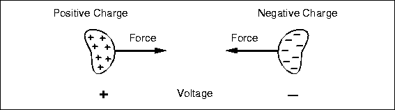
Specifically, bodies with opposite charges attract, they exert a force on each
other pulling them together. The magnitude of the force is proportional to the product of
the charge on each mass. This is just like gravity, where we use the term "mass"
to represent the quality of bodies that results in the attractive force that pulls them
together (see Fig. 4.1).
 |
Electrical force, like gravity, also depends inversely on the distance squared between the
two bodies; short separation means big forces. Thus it takes an opposing force to keep two
charges of opposite sign apart, just like it takes force to keep an apple from falling to
earth. It also takes work and the expenditure of energy to pull positive and
negative charges apart, just like it takes work to raise a big mass against gravity, or to
stretch a spring. This stored or potential energy can be recovered and put to work to do
some useful task. A falling mass can raise a bucket of water; a retracting spring can pull
a door shut or run a clock. It requires some imagination to devise ways one might hook on
to charges of opposite sign to get some useful work done, but it should be possible.
The potential that separated opposite charges have for doing work if they are released to fly together is called voltage, measured in units of volts (V). (Sadly, the unit volt is not named for Voltaire, but rather for Volta, an Italian scientist.) The greater the amount of charge and the greater the physical separation, the greater the voltage or stored energy. The greater the voltage, the greater the force that is driving the charges together. Voltage is always measured between two points, in this case, the positive and negative charges. If you want to compare the voltage of several charged bodies, the relative force driving the various charges, it makes sense to keep one point constant for the measurements. Traditionally, that common point is called "ground."
Early workers, like Coulomb, also observed that two bodies with charges of the same
type, either both positive or both negative, repelled each other (Fig. 4.2). They experience a force pushing
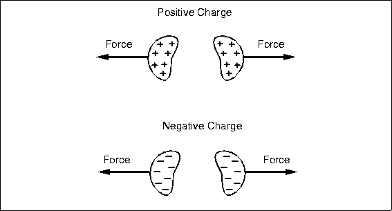 |
them apart, and an opposing force is necessary to hold them together, like holding a
compressed spring. Work can potentially be done by letting the charges fly apart, just
like releasing the spring. Our analogy with gravity must end here: no one has observed
negative mass, negative gravity, or uncharged bodies flying apart unaided. Too bad, it
would be a great way to launch a space probe. The voltage between two separated like
charges is negative; they have already done their work by running apart, and it
will take external energy and work to force them back together.
So how do you tell if a particular bunch of charge is positive or negative? You can't in isolation. Even with two charges, you can only tell if they are the same (they repel) or opposite (they attract). The names are relative; someone has to define which one is "positive." Similarly, the voltage between two points and , AB , is relative. If AB is positive you know the two points are oppositely charged, but you cannot tell if point has positive charge and point negative, or visa versa. However, if you make a second measurement between and another point , you can at least tell if and have the same charge by the relative sign of the two voltages, AB and AC to your common point . You can even determine the voltage between and without measuring it: BC = VAC - VAB . This is the advantage of defining a common point, like , as ground and making all voltage measurements with respect to it. If one further defines the charge at point to be negative charge, then a positive AB means point is positively charged, by definition. The names and the signs are all relative, and sometimes confusing if one forgets what the reference or ground point is.
Current
Charge is mobile and can flow freely in certain materials, called conductors. Metals and a few other elements and compounds are conductors. Materials that charge cannot flow through are called insulators. Air, glass, most plastics, and rubber are insulators, for example. And then there are some materials called semiconductors, that, historically, seemed to be good conductors sometimes but much less so other times. Silicon and germanium are two such materials. Today, we know that the difference in electrical behavior of different samples of these materials is due to extremely small amounts of impurities of different kinds, which could not be measured earlier. This recognition, and the ability to precisely control the "impurities" has led to the massive semiconductor electronics industry and the near-magical devices it produces, including those on your RoboBoard. We will discuss semiconductor devices later; now let us return to conductors and charges.
Imagine two oppositely charged bodies, say metal spheres, that are being held apart, as
in Fig. 4.3.
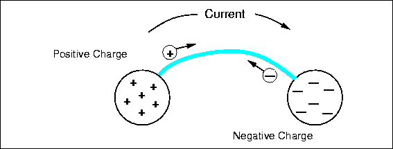 |
There is a force between them, the potential for work, and thus a voltage. Now we connect
a conductor between them, a metal wire. On the positively charged sphere, positive charges
rush along the wire to the other sphere, repelled by the nearby similar charges and
attracted to the distant opposite charges. The same thing occurs on the other sphere and
negative charge flows out on the wire. Positive and negative charges combine to neutralize
each other, and the flow continues until there are no charge differences between any
points of the entire connected system. There may be a net residual charge if the amounts
of original positive and negative charge were not equal, but that charge will be
distributed evenly so all the forces are balanced. If they were not, more charge would
flow. The charge flow is driven by voltage or potential differences. After things have
quieted down, there is no voltage difference between any two points of the system and no
potential for work. All the work has been done by the moving charges heating up the wire.
The flow of charge is called electrical current. Current is measured in amperes (a), amps for short (named after another French scientist who worked mostly with magnetic effects). An ampere is defined as a flow of one Coulomb of charge in one second past some point. While a Coulomb is a lot of charge to have in one place, an ampere is a common amount of current; about one ampere flows through a 100 watt incandescent light bulb, and a stove burner or a large motor would require ten or more amperes. On the other hand low power digital circuits use only a fraction of an ampere, and so we often use units of of an ampere, a milliamp, abbreviated as ma, and even of a milliamp, or a microamp, . The currents on the RoboBoard are generally in the milliamp range, except for the motors, which can require a full ampere under heavy load. Current has a direction, and we define a positive current from point to as the flow of positive charges in the same direction. Negative charges can flow as well, in fact, most current is actually the result of negative charges moving. Negative charges flowing from to would be a negative current, but, and here is the tricky part, negative charges flowing from to would represent a positive current from to . The net effect is the same: positive charges flowing to neutralize negative charge or negative charges flowing to neutralize positive charge; in both cases the voltage is reduced and by the same amount.
Batteries
Charges can be separated by several means to produce a voltage. A battery uses a chemical reaction to produce energy and separate opposite sign charges onto its two terminals. As the charge is drawn off by an external circuit, doing work and finally returning to the opposite terminal, more chemicals in the battery react to restore the charge difference and the voltage. The particular type of chemical reaction used determines the voltage of the battery, but for most commercial batteries the voltage is about 1.5 V per chemical section or cell. Batteries with higher voltages really contain multiple cells inside connected together in series. Now you know why there are 3 V, 6 V, 9 V, and 12 V batteries, but no 4 or 7 V batteries. The current a battery can supply depends on the speed of the chemical reaction supplying charge, which in turn often depends on the physical size of the cell and the surface area of the electrodes. The size of a battery also limits the amount of chemical reactants stored. During use, the chemical reactants are depleted and eventually the voltage drops and the current stops. Even with no current flow, the chemical reaction proceeds at a very slow rate (and there is some internal current flow), so a battery has a finite storage or shelf life, about a year or two in most cases. In some types of batteries, like the ones we use for the robot, the chemical reaction is reversible: applying an external voltage and forcing a current through the battery, which requires work, reverses the chemical reaction and restores most, but not all, the chemical reactants. This cycle can be repeated many times. Batteries are specified in terms of their terminal voltage, the maximum current they can deliver, and the total current capacity in ampere-hours.
You should handle batteries carefully, especially the ones we use in this course. Chemicals are a very efficient and compact way of storing energy. Just consider the power of gasoline or explosives, or the fact that you can play soccer for several hours powered only by a slice of cold pizza for breakfast. Never connect the terminals of a battery together with a wire or other good conductor. The battery we use for the RoboBoard is similar to the battery in cars, which uses lead and sulphuric acid as reactants. Such batteries can deliver very large currents through a short circuit, hundreds of amperes. The large current will heat the wire and possibly burn you; the resulting rapid internal chemical reactions also produce heat and the battery can explode, spreading nasty, reactive chemicals about. Charging these batteries with too large a current can have the same effect. Double check the circuit and instructions before connecting a battery to any circuit. More information on batteries can be found in Chapter 7.
Circuit Elements
Resistors
We need some way to control the flow of current from a voltage source, like a battery, so we do not melt wires and blow up batteries. If you think of current, charge flow, in terms of water flow, a good electrical conductor is like big water pipe. Water mains and fire hoses have their uses, but you do not want to take a drink from one. Rather, we use small pipes, valves, and other devices to limit water flow to practical levels. Resistors do the same for current; they resist the flow of charge; they are poor conductors. The value of a resistor is measured in ohms and represented by the Greek letter capital omega. There are many different ways to make a resistor. Some are just a coil of wire made of a material that is a poor conductor. The most common and inexpensive type is made from powdered carbon and a glue-like binder. Such carbon composition resistors usually have a brown cylindrical body with a wire lead on each end, and colored bands that indicate the value of the resistor. The key to reading these values is given in Chapter 2.
There are other types of resistors in your robot kit. The potentiometer is a variable resistor. When the knob of a potentiometer is turned, a slider moves along the resistance element. Potentiometers generally have three terminals, a common slider terminal, and one that exhibits increasing resistance and one that has decreasing resistance relative to the slider as the shaft is turned in one direction. The resistance between the two stationary contacts is, of course, fixed, and is the value specified for the potentiometer. The photoresistor or photocell is composed of a light sensitive material. When the photocell is exposed to more light, the resistance decreases. This type of resistor makes an excellent light sensor.
 
Ohm's Law
Ohm's law describes the relationship between voltage, , which is trying to force
charge to flow, resistance, , which is resisting that flow, and the actual resulting
current . The relationship is simple and very basic: ![]() .
Thus large voltages and/or low resistances produce large currents. Large resistors
limit current to low values. Almost every circuit is more complicated than just a battery
and a resistor, so which voltage does the formula refer to? It refers to the voltage
across the resistor, the voltage between the two terminal wires. Looked at another way,
that voltage is actually produced by the resistor. The resistor is restricting the flow of
charge, slowing it down, and this creates a traffic jam on one side, forming an excess of
charge with respect to the other side. Any such charge difference or separation results in
a voltage between the two points, as explained above. Ohm's law tells us how to calculate
that voltage if we know the resistor value and the current flow. This voltage drop is
analogous to the drop in water pressure through a small pipe or small nozzle.
.
Thus large voltages and/or low resistances produce large currents. Large resistors
limit current to low values. Almost every circuit is more complicated than just a battery
and a resistor, so which voltage does the formula refer to? It refers to the voltage
across the resistor, the voltage between the two terminal wires. Looked at another way,
that voltage is actually produced by the resistor. The resistor is restricting the flow of
charge, slowing it down, and this creates a traffic jam on one side, forming an excess of
charge with respect to the other side. Any such charge difference or separation results in
a voltage between the two points, as explained above. Ohm's law tells us how to calculate
that voltage if we know the resistor value and the current flow. This voltage drop is
analogous to the drop in water pressure through a small pipe or small nozzle.
Power
Current flowing through a poor conductor produces heat by an effect similar to
mechanical friction. That heat represents energy that comes from the charge traveling
across the voltage difference. Remember that separated charges have the potential to do
work and provide energy. The work involved in heating a resistor is not very useful,
unless we are making a hotplate; rather it is a byproduct of restricting the current flow.
Power is measured in units of watts (W), named after James Watt, the Englishman who
invented the steam engine, a device for producing lots of useful power. The power that is
released into the resistor as heat can be calculated as , where is the current
flowing through the resistor and is the voltage across it. Ohm's law relates these two
quantities, so we can also calculate the power as ![]() The
power produced in a resistor raises its temperature and can change its value or destroy
it. Most resistors are air-cooled and they are made with different power handling
capacity. The most common values are 1/8, 1/4, 1, and 2 watt resistors, and the bigger the
wattage rating, the bigger the resistor physically. Some high power applications use
special water cooled resistors. Most of the resistors on the RoboBoard are 1/8 watt.
The
power produced in a resistor raises its temperature and can change its value or destroy
it. Most resistors are air-cooled and they are made with different power handling
capacity. The most common values are 1/8, 1/4, 1, and 2 watt resistors, and the bigger the
wattage rating, the bigger the resistor physically. Some high power applications use
special water cooled resistors. Most of the resistors on the RoboBoard are 1/8 watt.
Combinations of Resistors
Resistors are often connected together in a circuit, so it is necessary to know how to
determine the resistance of a combination of two or more resistors. There are two basic
ways in which resistors can be connected: in series and in parallel. A
simple series resistance circuit is shown in Figure 4.4.
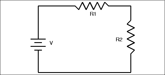
Determining the total resistance for two or more resistors in series is very simple. Total
resistance equals the sum of the individual resistances. In this case, T=R1+R2
. This makes common sense; if you think again in terms of water flow, a series of
obstructions in a pipe add up to slow the flow more than any one. The resistance of a
series combination is always greater than any of the individual resistors.
The other method of connecting resistors is shown in Figure 4.5, which shows a simple parallel resistance
circuit.
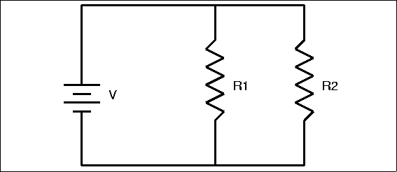
Our water pipe analogy indicates that it should be easier for current to flow through this
multiplicity of paths, even easier than it would be to flow through any single path. Thus,
we expect a parallel combination of resistors to have less resistance than any one of the
resistors. Some of the total current will flow through R1 and some will flow through R2,
causing an equal voltage drop across each resistor. More current, however, will flow
through the path of least resistance. The formula for total resistance in a parallel
circuit is more complex than for a series circuit:
| T={1 |
(1) |
Parallel and series circuits can be combined to make more complex structures, but the resulting complex resistor circuits can be broken down and analyzed in terms of simple series or parallel circuits. Why would you want to use such combinations? There are several reasons; you might use a combination to get a value of resistance that you needed but did not have in a single resistor. Resistors have a maximum voltage rating, so a series of resistors might be used across a high voltage. Also, several low power resistors can be combined to handle higher power. What type of connection would you use?
Capacitors
Capacitors are another element used to control the flow of charge in a circuit. The
name derives from their capacity to store charge, rather like a small battery. Capacitors
consist of two conducting surfaces separated by an insulator; a wire lead is connected to
each surface. You can imagine a capacitor as two large metal plates separated by air,
although in reality they usually consist of thin metal foils or films separated by plastic
film or another solid insulator, and rolled up in a compact package. Consider connecting a
capacitor across a battery, as in Fig. 4.6.
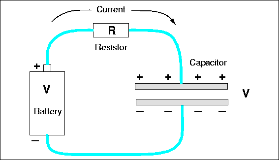
As soon as the connection is made charge flows from the battery terminals, along the wire
and onto the plates, positive charge on one plate, negative charge on the other. Why? The
like-sign charges on each terminal want to get away from each other. In addition to that
repulsion, there is an attraction to the opposite-sign charge on the other nearby plate.
Initially the current is large, because in a sense the charges can not tell immediately
that the wire does not really go anywhere, that there is no complete circuit of wire. The
initial current is limited by the resistance of the wires, or perhaps by a real resistor,
as we have shown in Fig. 4.6. But as
charge builds up on the plates, charge repulsion resists the flow of more charge and the
current is reduced. Eventually, the repulsive force from charge on the plate is strong
enough to balance the force from charge on the battery terminal, and all current stops.
Figure 4.7 shows how the current
might vary with
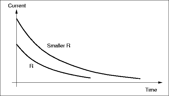 |
time for two different values of resistors. For a large resistor, the whole process is
slowed because the current is less, but in the end, the same amount of charge must exist
on the capacitor plates in both cases. The magnitude of the charge on each plate is equal.
The existence of the separated charges on the plates means there must be a voltage between the plates, and this voltage be equal to the battery voltage when all current stops. After all, since the points are connected by conductors, they should have the same voltage; even if there is a resistor in the circuit, there is no voltage across the resistor if the current is zero, according to Ohm's law. The amount of charge that collects on the plates to produce the voltage is a measure of the value of the capacitor, its capacitance, measured in farads (f). The relationship is , where Q is the charge in Coulombs. Large capacitors have plates with a large area to hold lots of charge, separated by a small distance, which implies a small voltage. A one farad capacitor is extremely large, and generally we deal with microfarads (), one millionth of a farad, or picofarads (pf), one trillionth -12) of a farad.
Consider the circuit of Fig. 4.6 again. Suppose we cut the wires after all current has stopped flowing. The charge on the plates is now trapped, so there is still a voltage between the terminal wires. The charged capacitor looks somewhat like a battery now. If we connected a resistor across it, current would flow as the positive and negative charges raced to neutralize each other. Unlike a battery, there is no mechanism to replace the charge on the plates removed by the current, so the voltage drops, the current drops, and finally there is no net charge left and no voltage differences anywhere in the circuit. The behavior in time of the current, the charge on the plates, and the voltage looks just like the graph in Fig. 4.7. This curve is an exponential function: . The voltage, current, and charge fall to about 37% of their starting values in a time of seconds, which is called the characteristic time or the time constant of the circuit. The time constant is a measure of how fast the circuit can respond to changes in conditions, such as attaching the battery across the uncharged capacitor or attaching a resistor across the charged capacitor. The voltage across a capacitor cannot change immediately; it takes time for the charge to flow, especially if a large resistor is opposing that flow. Thus, capacitors are used in a circuit to damp out rapid changes of voltage.
Combinations of Capacitors
Like resistors, capacitors can be joined together in two basic ways: parallel and series. It should be obvious from the physical construction of capacitors that connecting two together in parallel results in a bigger capacitance value. A parallel connection results in bigger capacitor plate area, which means they can hold more charge for the same voltage. Thus, the formula for total capacitance in a parallel circuit is:
| T=C1+C2...+Cn , | (2) |
the same form of equation for resistors in series, which can be confusing unless you think about the physics of what is happening.
The capacitance of a series connection is lower than any capacitor because for a given voltage across the entire group, there will be less charge on each plate. The total capacitance in a series circuit is
| T={1 |
(3) |
Again, this is easy to confuse with the formula for parallel resistors, but there is a nice symmetry here.
Inductors
Inductors are the third and final type of basic circuit component. An inductor is a coil of wire with many windings, often wound around a core made of a magnetic material, like iron. The properties of inductors derive from a different type of force than the one we invented charge to explain: magnetic force rather than electric force. When current flows through a coil (or any wire) it produces a magnetic field in the space outside the wire, and the coil acts just like any natural, permanent magnet, attracting iron and other magnets. If you move a wire through a magnetic field, a current will be generated in the wire and will flow through the associated circuit. It takes energy to move the wire through the field, and that mechanical energy is transformed to electrical energy. This is how an electrical generator works. If the current through a coil is stopped, the magnetic field must also disappear, but it cannot do so immediately. The field represents stored energy and that energy must go somewhere. The field contracts toward the coil, and the effect of the field moving through the wire of the coil is the same as moving a wire through a stationary field: a current is generated in the coil. This induced current acts to keep the current flowing in the coil; the induced current opposes any change, an increase or a decrease, in the current through the inductor. Inductors are used in circuits to smooth the flow of current and prevent any rapid changes.
The current in an inductor is analogous to the voltage across a capacitor. It takes time to change the voltage across a capacitor, and if you try, a large current flows initially. Similarly, it takes time to change the current through an inductor, and if you insist, say by opening a switch, a large voltage will be produced across the inductor as it tries to force current to flow. Such induced voltages can be very large and can damage other circuit components, so it is common to connect some element, like a resistor or even a capacitor across the inductor to provide a current path and absorb the induced voltage. (Often, a diode, which we will discuss later, is used.)
Inductors are measured in henrys (h), another very big unit, so you are more likely to see millihenries, and microhenries. There are almost no inductors on the RoboBoard, but you will be using some indirectly: the motors act like inductors in many ways. In a sense an electric motor is the opposite of an electrical generator. If current flows through a wire that is in a magnetic field (produced either by a permanent magnet or current flowing through a coil), a mechanical force will be generated on the wire. That force can do work. In a motor, the wire that moves through the field and experiences the force is also in the form of a coil of wire, connected mechanically to the shaft of the motor. This coil looks like and acts like an inductor; if you turn off the current (to stop the motor), the coil will still be moving through the magnetic field, and the motor now looks like a generator and can produce a large voltage. The resulting inductive voltage spike can damage components, such as the circuit that controls the motor current. In the past this effect destroyed a lot of motor controller chips and other RoboBoard components. The present board design contains special diodes that will withstand and safely dissipate the induced voltages -- we hope.
Combinations of Inductors
You already know how inductors act in combination because they act just like resistors. Inductance adds in series. This makes physical sense because two coils of wire connected in series just looks like a longer coil. Parallel connection reduces inductance because the current is split between the several coils and the fields in each are thus weaker.
Semiconductor Devices
The Truth About Charge
Our statements above about charge are not wrong, but they are simple and incomplete. In order to understand how semiconductor devices work one needs a more complete description of the nature of charge in the real world. Charge does not exist independently; it is carried by subatomic particles. For this discussion we will be concerned primarily with electrons, which carry a negative charge of -19 C , the minimum amount of charge that can exist in isolation. At least, no one has found any smaller amount than this fundamental quantum of charge.
Electrons are one component of atoms and molecules. Atoms are the building blocks out of which all matter is constructed. Atoms bond with each other to form substances. Substances composed of just one type of atom are called elements. For example, copper, gold and silver are all elements; that is, each of them consists of only one type of atom. More complex substances are made up of more than one atom and are known as compounds. Water, which has both hydrogen and oxygen atoms, is such a compound. The smallest unit of a compound is a molecule. A water molecule, for example, contains two hydrogen atoms and one oxygen atom.
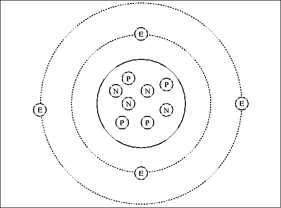
Atoms themselves are made up of even smaller components: protons, neutrons and electrons. Protons and neutrons form the nucleus of an atom, while the electrons orbit the nucleus. Protons carry positive charge and electrons carry negative charge; the magnitude of the charge for both particles is the same, one quantum charge, -19 C . Neutrons are not charged. Normally, atoms have the same number of protons and electrons and have no net electrical charge.
Electrons that are far from the nucleus are relatively free to move around under the influence of external fields because the force of attraction from the positive charge in the nucleus is weak at large distances. In fact, it takes little force in many cases to completely remove an outer electron from an atom, leaving an ion with a net positive charge. Once free, electrons can move at speeds approaching the speed of light (roughly 670 million miles per hour) through metals, gases and vacuum. They can also become attached to another atom, forming an ion with net negative charge.
Electric current in metal conductors consists of a flow of free electrons. Because
electrons have negative charge, the flow of electrons is in a direction opposite
to the positive current. Free electrons traveling through a conductor drift until they hit
other electrons attached to atoms. These electrons are then dislodged from their orbits
and replaced by the formerly free electrons. The newly freed electrons then start the
process anew. At the microscopic level, electron flow through a conductor is not a steady
stream, like water flowing from a faucet, but rather a series of short bursts.
Silicon
Semiconductor devices are made primarily of silicon (silicon's element symbol is
"Si"). Pure silicon forms rigid crystals because of its four valence (outermost)
electron structure -- one Si atom bonds to four other Si atoms forming a very
regularly shaped diamond pattern. Figure 4.10
shows part of a silicon crystal structure.
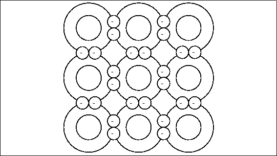
Pure silicon is not a conductor because there are no free electrons; all the electrons are
tightly bound to neighboring atoms. To make silicon conducting, producers combine or
"dope" pure silicon with very small amounts of other elements like boron or
phosphorus. Phosphorus has five outer valence electrons. When three silicon atoms and one
phosphorus atom bind together in the basic silicon crystal cell of four atoms, there is an
extra electron and a net negative charge. Figure4.11
shows the crystal structure of phosphorus doped silicon.
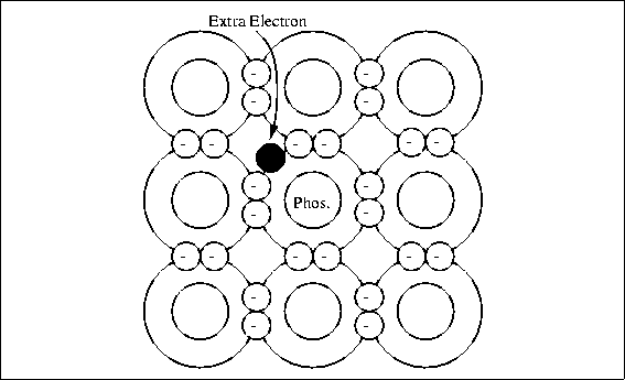
This type of material is called n-type silicon. The extra electron in the crystal cell is
not strongly attached and can be released by normal thermal energy to carry current; the
conductivity depends on the amount of phosphorus added to the silicon.
Boron has only three valance electrons. When three silicon atoms and one boron atom
bind with each other there is a "hole" where another electron would be if the
boron atom were silicon; see Fig. 4.12. This
gives the crystal cell a positive net charge (referred to as p-type silicon), and the
ability to pick up an electron easily from a neighboring cell.
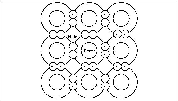
The resulting migration of electron vacancies or holes acts like a flow of positive charge
through the crystal and can support a current. It is sometimes convenient to refer to this
current as a flow of positive holes, but in fact the current is really the result of
electrons moving in the opposite direction from vacancy to vacancy.
Diodes
Both p-type and n-type silicon will conduct electricity just like any conductor; however, if a piece of silicon is doped p-type in one section and n-type in an adjacent section, current will flow in only one direction across the junction between the two regions. This device is called a diode and is one of the most basic semiconductor devices.
A diode is called forward biased if it has a positive voltage across it from
from the p- to n-type material. In this condition, the diode acts rather like a good
conductor, and current can flow, as in Fig. 4.13.
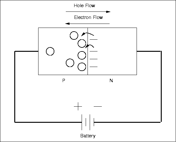
There will be a small voltage across the diode, about 0.6 volts for Si, and this
voltage will be largely independent of the current, very different from a resistor.
If the polarity of the applied voltage is reversed, then the diode will be reverse
biased and will appear nonconducting (Fig. 4.14).
Almost no current will flow and there will be a large voltage across the device.
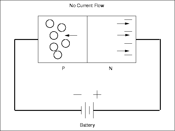
The non-symmetric behavior is due to the detailed properties of the pn-junction. The diode
acts like a one-way valve for current and this is a very useful characteristic. One
application is to convert alternating current (AC), which changes polarity periodically,
into direct current (DC), which always has the same polarity. Normal household power is AC
while batteries provide DC, and converting from AC to DC is called rectification. Diodes
are used so commonly for this purpose that they are sometimes called rectifiers, although
there are other types of rectifying devices. Figure 4.15 shows the input and output current for a
simple half-wave
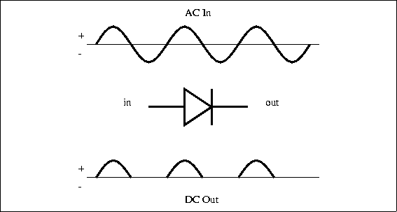
rectifier. The circuits gets its name from the fact that the output is just the positive
half of the input waveform. A full-wave rectifier circuit (shown in Figure 4.16) uses four diodes arranged so that both
polarities of the input waveform can be used at the output.
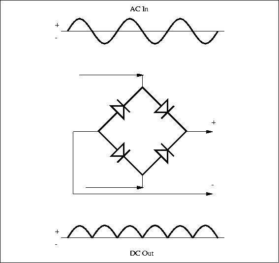
The full-wave circuit is more efficient than the half-wave one.

FET Current Source
FET constant current sources use JFETs and MOSFETs to deliver a load current which remains constant despite changes in load resistance or supply voltage


0 Comments